seki lab. logo

Research
研究内容

Measurement
測定

Intrinsic Charge Carrier Mobility Probed by Microwaves

Charge carrier mobility is an essential parameter providing control over the performance of semiconductor devices fabricated using a variety of organic molecular materials.
Recent design strategies toward molecular materials have been directed at the substitution of amorphous silicon-based semiconductors; accordingly, numerous measurement techniques have been designed and developed to probe the electronic conducting nature of organic materials bearing extremely wide structural variations in comparison with inorganic and/or metal-oxide semiconductor materials.
In the present project, we have developped non-contact measurement technique with microwave probes (TIme-Resolved Microwave Conductivity Measurement, TRMC) as a versatile tool for charge carrier mobility in organic molecules, crystals, and supramolecular assemblies for semiconductor applications.
Beyond the simple substitution of amorphous silicon, we have attempted to address the systematic use of measurement techniques for future development of organic molecular semiconductors.

Keyword

Semiconductors, Microwave, Mobility, Effective Mass, Charge Carrier Transport

References

S. Seki, A. Saeki, T. Sakurai and D. Sakamaki
Charge carrier mobility in organic molecular materials probed by electromagnetic waves
Phys. Chem. Chem. Phys., 16, 11093-11113(2014). DOI: 10.1039/c4cp00473f
A. Saeki, Y. Koizumi, T. Aida, and S. Seki
Comprehensive Approach to Intrinsic Charge Carrier Mobility in Conjugated Organic Molecules, Macromolecules, and Supramolecular Architectures
Acc. Chem. Res., 45, 1193-1202(2012). DOI: 10.1021/ar200283b

Development of Non-Contact Non-Destructive Technique to Evaluate Charge Carrier Transport at Semiconductor-Insulator Interfaces

In most organic electronic devices, charge carriers are transported during device operation at the material interfaces such as electrode/semiconductor, insulator/semiconductor, and semiconductor/semiconductor.
However, analytical tools to address interfacial carrier transporting phenomena have been less developed.
Here we successfully developed a novel technique named field-induced time-resolved microwave conductivity (FI-TRMC) for the evaluation of charge carrier mobility at the insulator/semiconductor interfaces without grain boundary effects.
In this method, we introduce a simple metal-insulator-semiconductor (MIS) device into the microwave cavity, where the charge carrier generation takes place at the insulator-semiconductor interface by applying a gate bias and charge carrier motions are probed by reflected microwave changes.

Keyword

Organic Semiconductor, Insulator, Interface, Charge Carrier Transport

References

W. Choi, T. Miyakai, T. Sakurai, A. Saeki, M. Yokoyama, and S. Seki
Non-contact, non-destructive, quantitative probing of interfacial trap sites for charge carrier transport at semiconductor-insulator boundary
Appl. Phys. Lett., 105, 33302(2014). DOI: 10.1063/1.4891052
Y. Honsho, T. Miyakai, T. Sakurai, A. Saeki, and S. Seki
Evaluation of Intrinsic Charge Carrier Transport at Insulator-Semiconductor Interfaces Probed by a Non-Contact Microwave-Based Technique
Sci. Rep., 3, 3182(2013). DOI: 10.1038/srep03182

π-Molecular Figuration under Ultra-High Pressure with Unique Electronic Properties Probed by Combined Electromagnatic Wave Spectroscopy

Continuous tuning of conjugated molecular design toward the optimized inter-molecular stacking and assemblies is an essential prerequisite to unveil the inherent electrical and optical features of organic electronics.
This is also the case for the modulation of backbone conformation and interchain distance of conjugated polymers, aiming their application to "plastic electronics."
To this end, applying pressure in a hydrostatic medium or diamond anvil cell is a facile approach without the need for synthetic molecular engineering of conjugated molecules / polymers.
Here we have developped high-pressure, time-resolved microwave conductivity (HP-TRMC) for evaluation of transient photoconductivity in conjugated polymeric materials.
X-ray diffraction experiments under high pressure were performed to detail the pressure dependence of backbone configuration of conjugated polymer materials as well as phase and molecular stacking structures of molecular assemblies.
The HP-TRMC results are further correlated with high-pressure Raman spectroscopy and density functional theory calculation.
A mechanistic insight into the interplay of intra- and intermolecular mobilities is a key to tailoring the dynamic π-figuration associated with electrical properties, which may lead to the use of HP-TRMC in exploring divergent π-conjugated materials at the desired molecular arrangement and conformation.

Keyword

Ultra-high Pressure, Microwave, Modulation, Microwave, Raman Spectroscopy

References

Y. Noguchi, A. Saeki, T. Fujiwara, S. Yamanaka, M. Kumano, T. Sakurai, N. Matsuyama, M. Nakano, N. Hirao, Y. Ohishi, and S. Seki
Evaluation of Pressure Modulation of Backbone Conformation and Intermolecular Distance of Conjugated Polymers Toward Understanding the Dynamism of π-Figuration of their Conjugated System
J. Phys. Chem. B, 119, 7219-7230(2015). DOI: 10.1063/1.4891052

Synthetic
合成

Design of Novel Organic Semiconductors Utilizing Unique Molecular Shapes

Because of the varieties of molecular designs for organic molecules, many kinds of organic semiconductors based on π-conjugated systems have been reported in recent years.
In this study, we focus on the design of unique organic semiconducting molecules, macromolecules, and their blends that can realize novel functions or propose new concepts.
For example, by using specific macromolecules called "Shish-kebab" polymers featuring one-dimensionally connected phthalocyanine arrays together with electron-accepting molecules, we have developed electron donor-acceptor segregated nanostructures showing high photoconductivity.

Keyword

Organic Semiconductor, π-Conjugated Molecules, Self-Assembly, Photoconductivity, Microwave

References

S. Yoneda, T. Sakurai, T. Nakayama, K. Kato, M. Takata, and S. Seki
Systematic Studies on Side-Chain Structures of Phthalocyaninato-Polysiloxanes: Polymerization and Self-Assembling Behaviors
J. Porphyrins Phthalocyanines, 19, 160–170(2015). DOI: 10.1142/S1088424614501053

Microwave-Based Evaluation of Intrinsic Charge Carrier Mobility for Charge Transporting Materials

Our group has joint research projects with other groups that focus on the development of new materials.
By means of our FP- or FI-TRMC techniques as well as transient absorption spectroscopy, we evaluated charge carrier transporting property of such newly-developed materials.
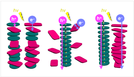
As recent representative works, for example, we evaluated, through FP-TRMC/TAS combined method, the charge carrier mobility of polyrotaxane-based materials composed of semiconducting phenylene-ethynylene wires isolated by insulating cyclodextrin covers.
Self-assembled polymers and supramolecular materials are of interest for our study of clarifying the relationship between structure and semiconducting property.
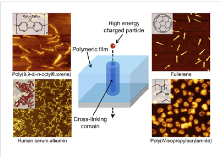
On the other hand, by using FI-TRMC technique, we studied the local-scale charge carrier mobility of π-extended acene- and heteroacene-based thin films at the semiconductor–insulator interfaces.
Furthermore, recently we tried to evaluate the charge carrier transporting property of MOFs, COFs, and PCPs that have not been used for semiconductors.
In particular, crystalline thin films developed by crystal growth on substrates are the potential targets for the precise evaluation.

Keyword

Organic Semiconductor, π-Conjugated Molecules, Microwave, Charge Carrier Mobility, One-Dimensional, Two-Dimensional

References

J. Terao, A. Wadahama, A. Matono, T. Tada, S. Watanabe, S. Seki, T. Fujihara, and Y. Tsuji
Design principle for increasing charge mobility of π-conjugated polymers using regularly localized molecular orbitals
Nature Commun., 4, 1691(2013). DOI: 10.1038/ncomms2707
T. Mondal, T. Sakurai, S. Yoneda, S. Seki, and S. Ghosh
Semiconducting Nanotubes by Intrachain Folding Following Macroscopic Assembly of a Naphthalene-Diimide (NDI) Appended Polyurethane
Macromolecules, 48, 879-888(2015). DOI: 10.1021/ma502410d
Y. Tsutsui, T. Sakurai, S. Minami, K. Hirano, T. Satoh, W. Matsuda, K. Kato, M. Takata, M. Miura and S. Seki
Evaluation of Intrinsic Charge Carrier Transporting Properties of Linear- and Bent-Shaped π-Extended Benzo-Fused Thieno[3,2-b]thiophenes
Phys. Chem. Chem. Phys., 17, 9624-9628(2015). DOI: 10.1039/C5CP00785B
J. Guo, Y. Xu, S. Jin, L. Chen, T. Kaji, Y. Honsho, M. A. Addicoat, J. Kim, A. Saeki, H. Ihee, S. Seki, S. Irle, M. Hiramoto, J. Gao, and D. Jiang
Conjugated organic framework with three-dimensionally ordered stable structure and delocalized π clouds" Nature Commun.
J. Mater. Chem. C, 4, 2736(2013). DOI: 10.1038/ncomms3736
J. Liu, W. Zhou, J. Liu, I. Howard, G. Kilibarda, S. Schlabach, D. Coupry, M. Addicoat, S. Yoneda, Y. Tsutsui, T. Sakurai, S. Seki, Z. Wang, P. Lindemann, E. Redel, T. Heine, and C. Wöll
Photoinduced Charge Carrier Generation in Epitaxial MOF Thin Films: High Efficiency as a Result of an Indirect Band Gap?
Angew. Chem. Int. Ed., 54, 7441-7445(2015). DOI: 10.1002/anie.201501862
L. Sun, T. Miyakai, S. Seki, and M. Dinca
Mn2(2,5-disulfhydrylbenzene-1,4-dicarboxylate): A Microporous Metal−Organic Framework with Infinite (−Mn−S−)∞ Chains and High Intrinsic Charge Mobility
J. Am. Chem. Soc., 135, 8185-8188(2013). DOI: 10.1021/ja4037516

Nanowires
ナノワイヤ

Fabrication of functional nanowires by single particle nano-fabrication technique

Single particle nano-fabrication technique (SPNT) as a fabrication method of nano-structures was established in our laboratory.
High-energy charged particles (ion beam) induced a non-homogeneous cross-linking reaction in the nanometer-scale cylindrical area of the polymer films along their trajectories.
Development of irradiated samples using good solvents to remove a non-cross-linked polymer afforded nanowires.
The length, thickness and number density of the fabricated nanowire can be controlled by changing several parameters for the incident ion beam.
Application of this technique for functional polymers such as conductive polymers and biopolymers is expected to be very effective for fabrication of various functional nanowires.

Keyword

High Energy Particle, Nanowire, Cross-linking, Ion beam

References

K. Kamiya, K. Kayama, M. Nobuoka, S. Sakaguchi, T. Sakurai, M. Kawata, Y. Tsutsui, M. Suda, A. Idesaki, H. Koshikawa, M. Sugimoto, G. B. V. S. Lakshmi, D. K. Avasthi, S. Seki
Ubiquitous organic molecule-based free-standing nanowires with ultra-high aspect ratios
Nature Commun., 12, 4025(2021). DOI: 10.1038/s41467-021-24335-x
H. L. Cheng, M. T. Tang, W. Tuchinda, K. Enomoto, A. Chiba, Y. Saito, T. Kamiya, M. Sugimoto, A. Saeki, T. Sakurai, M. Omichi, D. Sakamaki, and S. Seki
Reversible Control of Radius and Morphology of Fluorene-Azobenzene Copolymer Nanowires by Light Exposure
Adv. Mater. Interfaces, 2, 1400450(2015). DOI: 10.1002/admi.201400450
M. Omichi, A. Asano, S. Tsukuda, K. Takano, M. Sugimoto, A. Saeki, D. Sakamaki, A. Onoda, T. Hayashi, and S. Seki
Fabrication of enzyme-degradable and size-controlled protein nanowires using single particle nano-fabrication technique
Nature. Commun., 5, 3718(2014). DOI: 10.1038/ncomms4718
Y. Maeyoshi, A. Saeki, S. Suwa, M. Omichi, H. Marui, A. Asano, S. Tsukuda, M. Sugimoto, A. Kishimura, K. Kataoka, and S. Seki
Fullerene nanowires as a versatile platform for organic electronics
Sci. Rep., 2, 600/1-6(2012). DOI: 10.1038/srep00600